
Over Voltage Protection and Lock Out for 5 V, 3.3 V, and 12 V
Under Voltage Protection and Lock Out for 5 V and 3.3 V
Fault Protection Output with Open Drain Output Stage
Open Drain Power Good Output Signal for Power Good Input, 5 V and 3.3 V
300 ms Power Good Delay
75 ms Delay for 5-V and 3.3-V Short-Circuit Turn On Protection
38 ms PSON Control Debounce
73 ms Width Noise Deglitches
Wide Power Supply Voltage Range from 4 V to 15 V
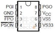
D OR P PACKAGE
(TOP VIEW)
description:
The TPS5510 is designed to minimize external components of personal computer switching power supply systems. It provides protection circuits, power good indicator, fault protection output (FPO), and a PSON control.
OVP (Over Voltage Protection) monitors 5 V, 3.3 V, and 12 V (12 V OV detects via VCC terminal). UVP (Under Voltage Protection) monitors 5 V and 3.3 V. When an OV or UV condition is detected, the PGO (power good output) is asserted low and FPO is latched high. PSON from low to high resets the protection latch. UVP function will be enabled 75 ms after PSON is set low and debounced.
Power good feature monitors PGI, 5 V and 3.3 V and issues a power good signal when they are ready.
The TPS5510 is characterised for operation from TJ = –40°C to 125°C junction temperature.

Figure 1. TPS5510 Typical Application

functional block diagram

Terminal Functions
