The AD587 represents a major advance in the state-of-the-art in monolithic voltage references. Using a proprietary ion-implanted buried Zener diode and laser wafer trimming of high stability thin-film resistors, the AD587 provides outstanding perfor-mance at low cost.
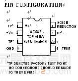
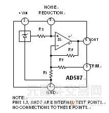
The AD587 offers much higher performance than most other 10 V references. Because the AD587 uses an industry standard pinout, many systems can be upgraded instantly with the AD587. The buried Zener approach to reference design pro-vides lower noise and drift than bandgap voltage references. The AD587 offers a noise reduction pin which can be used to further reduce the noise level generated by the buried Zener.
The AD587 is recommended for use as a reference for 8-, 10-,12-, 14- or 16-bit D/A converters which require an external precision reference. The device is also ideal for successive approximation or integrating A/D converters with up to 14 bits of accuracy and, in general, can offer better performance than the standard on-chip references.
The AD587J, K and L are specified for operation from 0°C to +70°C, and the AD587S, T and U are specified for –55°C to +125°C operation. All grades are available in 8-pin cerdip. The J and K versions are also available in an 8-pin Small Outline IC(SOIC) package for surface mount applications, while the J, K,and L grades also come in an 8-pin plastic package.
REV. D
Information furnished by Analog Devices is believed to be accurate and reliable. However, no responsibility is assumed by Analog Devices for its use, nor for any infringements of patents or other rights of third parties which may result from its use. No license is granted by implication or otherwise under any patent or patent rights of Analog Devices.
AD587JR产品
1. Laser trimming of both initial accuracy and temperature coefficients results in very low errors over temperature with-out the use of external components. The AD587L has a maximum deviation from 10.000 V of ±8.5 mV between 0°C and +70°C, and the AD587U guarantees ±14 mV maximum total error between –55°C and +125°C.
2. For applications requiring higher precision, an optional fine trim connection is provided.
3. Any system using an industry standard pinout 10 volt refer-ence can be upgraded instantly with the AD587.
4. Output noise of the AD587 is very low, typically 4 µV p-p. A noise reduction pin is provided for additional noise filtering using an external capacitor.
5. The AD587 is available in versions compliant with MIL-STD-883. Refer to the Analog Devices Military Products Databook or current AD587/883B data sheet for detailed specifications
AD587JR最大额定值
VIN to Ground . . . . . . . . . . . . . . . . . . . . . . . . . . . . . 36 V
Power Dissipation (+25°C) . . . . . . . . . . . . . . . . 500 mW
Storage Temperature . . . . . . . . . . . . . . –65°C to +150°C
Lead Temperature (Soldering, 10 sec) . . . . . . . +300°C
Package Thermal Resistance
èJC . . . . . . . . . . . . . . . . . . . . . . . . . . . . . . 22°C/W
èJA . . . . . . . . . . . . . . . . . . . . . . . . . . . . . . 110°C/W
Output Protection: Output safe for indefinite short to ground and momentary short to VIN.